開催予定
展示会
東京ビックサイト2025.12.17 - 19 (JPN)
【出展のお知らせ】Matlantis、SEMICON Japan 2025 に共同出展します
Matlantis Corporation will be co-exhibiting with Preferred Networks (PFN) at SEMICON Japan 2025, which will be held at Tokyo Big Sight from Wednesday, December 17th to Friday, December 19th, 2025.
SEMICON Japan is one of Japan's largest international exhibitions, bringing together the entire semiconductor supply chain, including semiconductor devices, manufacturing equipment, materials, and packaging technologies. It is known as an annual end-of-year event, where numerous companies, research institutes, engineers, and researchers from Japan and overseas participate, allowing visitors to experience the latest trends in next-generation semiconductor technology.
Matlantis provides AI simulation technology to understand, design, and optimize the materials that underpin semiconductor device performance and processes at the atomic level.
As semiconductors continue to shrink and become more sophisticated, it is becoming more important than ever to precisely understand material reactivity, interface behavior, and thin film formation mechanisms. Matlantis predicts these complex material phenomena quickly and accurately, bringing new approaches to process development and material discovery.
Booth Information
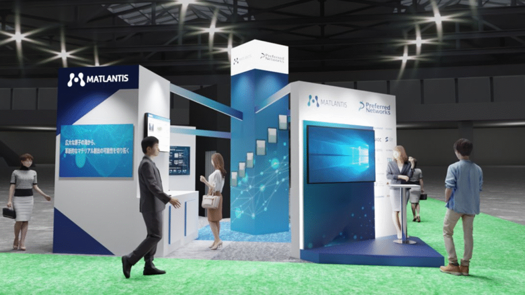
Booth location: West Exhibition Hall 1F West Atrium A1322
Dates: Wednesday, December 17, 2025 - Friday, December 19, 2025 10:00-17:00
venue: Tokyo Big Sight
(West Atrium AI x Sustainability x Semiconductor Summit)
Venue map:https://www.semiconjapan.org/jp/exhibits/floor-map/floor-map-pdf
Visitor registration: https://www.semiconjapan.org/jp/about/pricing-and-register
Exhibition contents
- Introducing customer cases using Matlantis
- Introduction of examples of materials exploration in the semiconductor industry (surface reactions, interface behavior, thin film formation, etc.)
- Consultation on applicability to research themes
Our engineers will provide individual guidance on how much of your research topic, such as surface reactions, interface behavior, and material exploration, can be reproduced and calculated with Matlantis.
Mini Seminar
At the booth, we will be holding mini seminars from time to time to briefly introduce specific calculation examples of semiconductor process analysis and material exploration using Matlantis (the schedule will be announced at the booth on the day).
We look forward to seeing you all there.
公開日:2025.12.15
-


 URL
URL
Copied
新着イベント・セミナー
NEW
過去のお知らせ
ウェビナー
オンライン2025.12.12 (JPN)
プロセスインフォマティクスセミナーに登壇|汎用機械学習ポテンシャルで刷新する材料開発

NEW
過去のお知らせ
学会・講演会
Pacifico Yokohama・ JPN2025.12.8 - 13
Matlantis will be speaking at MRM2025 @ Pacifico Yokohama
NEW
過去のお知らせ
学会・講演会
Hynes Convention Center2025.11.30-12.5 (USA)
2025 MRS Fall Meeting & Exhibit発表および出展のお知らせ

過去のお知らせ
ウェビナー
Online (Zoom)2025.12.9
[Webinar] Matlantis: Universal Atomistic Simulation for AI-Driven Materials Discovery
過去のお知らせ
学会・講演会
Hynes Convention Center2025.11.2-6 (USA)
Announcement of presentations and exhibits at the 2025 AIChE Annual Meeting