Matlantis has signed a Joint Development Project (JDP) agreement with imec, a world-leading global center for advanced semiconductor research and innovation. Together, we will explore how Matlantis PFP, the universal machine-learning interatomic potential at the core of the atomistic simulator Matlantis™, can be applied to nanoelectronics materials challenges proposed by imec. In this post, I would like to share why this theme matters and what the project will cover.
As generative AI spreads, demand for computing is growing rapidly. Semiconductors, which carry out that computing, have long gained performance through the miniaturization of circuits. But miniaturization alone is becoming harder to rely on, and new structures and materials are being introduced. This puts renewed focus on the materials themselves and on the manufacturing processes that shape them.
This is where Matlantis works: the development of materials and processes. Atomistic simulation can be used not only to search for new materials, but also to understand what happens at surfaces and interfaces during manufacturing processes such as deposition and etching. We believe that accelerating development on both fronts, materials and processes, helps underpin the progress of semiconductors.
1. Why interfaces are hard to simulate
Improving chip performance increasingly requires connecting chips to each other at finer pitches and with far more connections. Hybrid bonding is becoming central to the 3D integration of chips, and its reliability depends on what happens at the atomic level where two materials meet.
These interfaces, and the multi-element amorphous materials used in advanced devices, are hard to model: quantum-mechanical methods are accurate but too slow for realistic system sizes.
PFP is a universal machine-learning interatomic potential trained on a broad and diverse set of atomic structures. It predicts the energies and atomic forces of a structure at a fraction of the computational cost typically associated with first-principles methods such as density functional theory (DFT).
2. What we will work on together
The project, named SIMPL (Simulations with Machine-Learning Potentials), explores how PFP can help close the gap between accuracy and speed. It consists of two work packages.
Evaluating PFP. Imec will evaluate how well PFP reproduces atomic forces and energies on a range of nanoelectronics-relevant materials and interfaces chosen by imec.
Modeling hybrid bonding adhesion.We will study adhesion between amorphous dielectrics and polycrystalline metals, to better understand the mechanisms behind hybrid bonding and to support more efficient hybrid bonding techniques for 3D packaging in nanoelectronics.
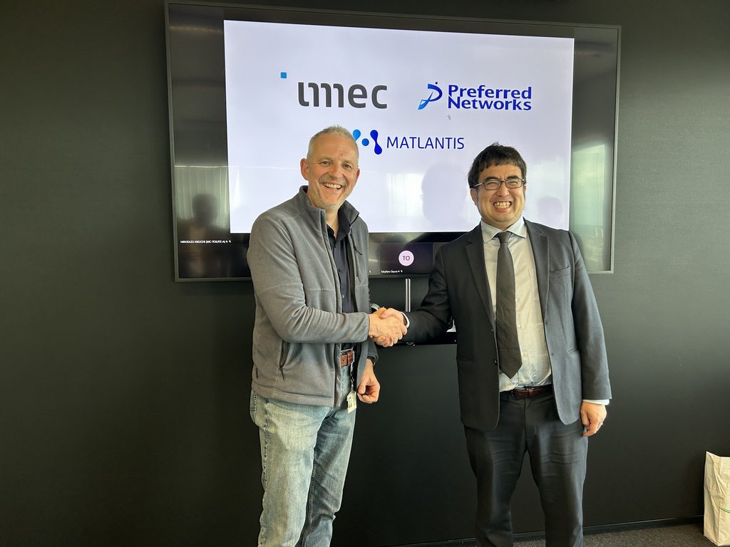
Right: Daisuke Okanohara, CEO, Matlantis
3. Comments from imec and Matlantis
Geoffrey Pourtois, imec Fellow, commented:
“At imec, we work at the forefront of semiconductor innovation, developing the technologies that will enable future generations of chips. Understanding material behaviour at the atomic level is essential to this progress. The collaboration with Matlantis will enable us to explore how machine-learning-based atomistic simulation can accelerate this understanding and support the development of advanced technologies such as hybrid bonding. We are excited to work together and turn these insights into new opportunities for semiconductor innovation.”
Daisuke Okanohara, CEO of Matlantis, commented:
“Imec is one of the world’s foremost research and innovation hubs, bringing together researchers from universities and companies around the globe to pioneer next-generation semiconductor technologies.
As semiconductor technology advances, understanding and exploring materials at the atomic level is becoming increasingly important. Through this collaboration, we aim to apply the AI-driven materials simulation technology that Matlantis has developed to cutting-edge semiconductor research, accelerating the discovery of new materials and the pace of R&D.
Through this collaboration, we look forward to further expanding the possibilities of AI-driven materials development for researchers worldwide.”
4. Looking ahead
We are deeply grateful to imec for this opportunity. We will make the most of this collaboration and hope it leads to breakthroughs in materials development.
-


 URL
Copied
New Articles
NEW
How Do Materials Engineers in Japan View Computational Chemistry and Materials Informatics? – A survey of 82 R&D professionals reveals a gap that splits the field in two

Materials Informatics computational chemistry

NEW
The Lab Is (Not) All You Need: Why autonomous laboratories make atomistic simulation more valuable, not less

Lab Automation Machine Learning Interatomic Potentials
The front runner of AI for Science – A Report from the "Matlantis User Conference 2026"
Conference Report

Changing the rules of materials development with Physics-Grounded AI: how Matlantis PFP came to be

Interview

Benchmarking Matlantis-PFP v9 on MLIP Arena (full version)