
Blog
We provide easy-to-understand explanations of Matlantis terminology and the latest technology trends from an expert's perspective. We deliver information that will help you solve your problems and make new discoveries.
Editor’s PICK
How to Choose Molecular Dynamics (MD) Simulation Software: 6 Key Points and 14 Tools Compared

In the field of materials development, we often encounter atomic-level questions such as, "Why do ions diffuse so easily in this material?", "What is happening near the interface?", and "How do defects affect the properties?". A powerful tool for answering these questions is molecular dynamics (MD) simulation, which visualizes the movement of atoms and molecules through calculations.
Molecular Dynamics Explainer

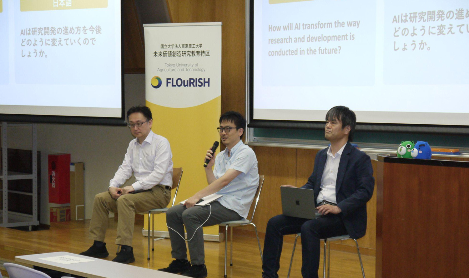
[Presentation Report] Tokyo University of Agriculture and Technology Doctor's Café #37 & AI Salon #14
"Interdisciplinary Innovation through AI ~Challenges to Sustainable Materials Development~" Event details: https://www.tuat-flourish.jp/topics/event/3832/ July 22, 2026, Tokyo University of Agriculture and Technology, Future Value Creation Research and Education Special Zone (FLOuRISH) presents "Doctor's Café #37 & AI Salon #14" (Kogane
Conference Report
Micro-Physical AI: Another invisible form of physical AI and the future of materials development

What is Physical AI? Current LLMs (Large Language Models) learn about the world from text. Through this, they incorporate the knowledge accumulated by humans so far and are already having a major impact on the world. However, to borrow Plato's words, text is merely a "shadow" of reality. Text only records a portion of what humans have been able to verbalize, and the overwhelming majority of phenomena occurring in the physical world have not yet been turned into words.
CEO Blog
What is the semiconductor manufacturing process? A thorough explanation of front-end processes such as film deposition, photoetching, and CMP from a materials simulation perspective.

Semiconductor devices are manufactured by forming nanoscale structures on silicon wafers. This involves repeating numerous processes such as film deposition, photolithography, etching, ion implantation, and planarization to create fine circuit structures on the wafer. In these manufacturing processes, the physical properties of the materials and the reactions occurring at the surface and interface significantly impact device performance and yield. In recent years, the micro-scale of devices has been a key factor.
Explainer computational chemistry
AI pioneers materials development through computational chemistry

This article is a blog post based on an article written by Zhang, Customer Success Engineer Matlantis Corporation, which was published in the February 2026 issue of the technical magazine "Monthly Material Stage" in the special feature "Improving the Efficiency of Materials Development Using AI and Automated Experiments." 1. Materials Development to Date Our lives have been enriched by numerous innovative materials. However,
DFT Molecular Dynamics Machine Learning Interatomic Potentials Explainer
Featured Tags
Blog article list
NEW
Benchmarking Matlantis-PFP v9 on MLIP Arena (full version)

NEW
Introducing Matlantis-PFP v9: Benchmarking on MLIP Arena and Improving Experimental Agreement with r2SCAN
NEW
How to Choose Molecular Dynamics (MD) Simulation Software: 6 Key Points and 14 Tools Compared
Molecular Dynamics Explainer
[Presentation Report] Tokyo University of Agriculture and Technology Doctor's Café #37 & AI Salon #14
Conference Report
Micro-Physical AI: Another invisible form of physical AI and the future of materials development
CEO Blog
What is lab automation? Concepts and latest trends in experimental automation in materials development.
Lab automation Explainer
What is the semiconductor manufacturing process? A thorough explanation of front-end processes such as film deposition, photoetching, and CMP from a materials simulation perspective.
Explainer computational chemistry
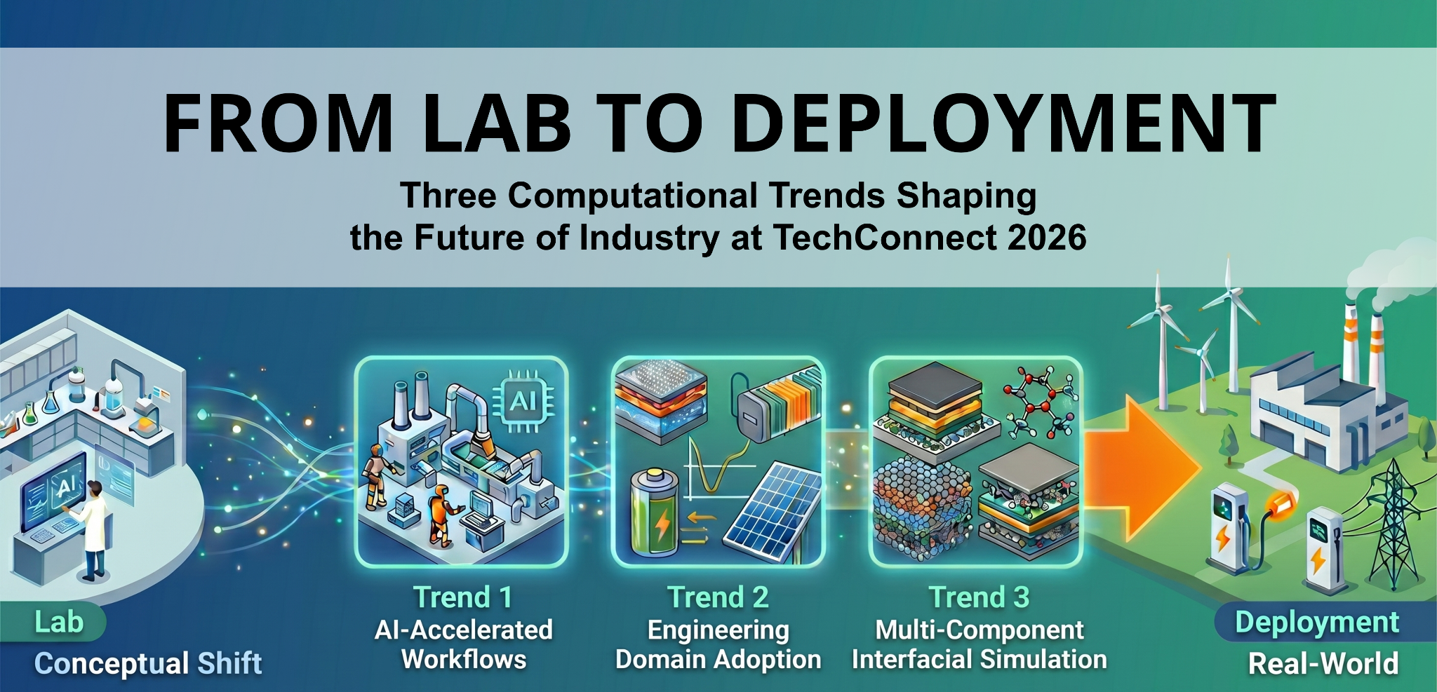
From Lab to Application: Three Computational Trends Shaping the Future of Industry, as Seen at TechConnect 2026

Conference Report
Three Computational Trends Reshaping Materials Science from TMS 2026

Conference Report
What Is Digital Transformation in Materials R&D? Accelerating Materials Discovery
Materials Informatics computational chemistry
Crystal Structure Prediction Using Optuna in Matlantis CSP
AI pioneers materials development through computational chemistry
DFT Molecular Dynamics Machine Learning Interatomic Potentials Explainer
- Go to the first page
- Previous page
- 1
- 2
- 3
- Next page
- To the last page
-


 URL
URL
Copied
