
Semiconductor devices are manufactured by forming nanoscale structures on silicon wafers. This process involves repeating numerous steps, such as film deposition, photolithography, etching, ion implantation, and planarization, to create intricate circuit structures on the wafer.
In these manufacturing processes, the physical properties of materials and the reactions that occur at their surfaces and interfaces significantly influence device performance and yield. In recent years, as devices have become smaller, there are increasing instances where the nanoscale behavior of materials determines the success or failure of the process.
However, many of these phenomena are difficult to understand in detail through experiments alone, and the importance of methods for analyzing material behavior at the atomic level is increasing. For this reason, in recent years, research using material simulations to understand surface reactions and material behavior has become widespread.
This article provides an overview of the "front-end" processes within the semiconductor manufacturing process from the perspective of materials simulation. First, we will clarify what a semiconductor is and how devices are made, and then introduce the purpose, technical challenges, and materials research being conducted at each stage of the process.
What you will learn from this article
- What is a semiconductor? Understanding its basic structure, including wafers, dies, and wiring layers.
- The difference between front-end and back-end processes in semiconductor manufacturing
- The role of the front-end process (film deposition, photolithography, etching, ion implantation, annealing, CMP, cleaning)
- What difficulties have arisen in each process due to miniaturization?
- How are material simulations being used in each process? (Calculation examples)
- Examples of semiconductor simulation applications in companies and research institutions (paper introductions)
table of contents
- What are semiconductors?
- Front-End vs. Back-End Processes
- Deposition, the process of creating a film using atoms, is...
- Photolithography is a technique for transferring circuit patterns.
- Etching is the process of removing unwanted material.
- Ion Implantation: Controlling Electrical Properties
- What is CMP, which flattens surfaces?
- Cleaning that controls surface condition
- Examples of research and development utilizing materials simulations by companies
What are semiconductors?

Semiconductor structure image
A semiconductor is a material that possesses properties intermediate between those of a conductor, which conducts electricity well, and an insulator, which conducts very little electricity. Because of these properties, it is called a semiconductor, meaning "a material that is neither a conductor nor an insulator, but has properties in between." A typical example is silicon, and this property is used to create electronic components that control the flow of electric current.
In semiconductor devices, structures to control this flow of current are fabricated on the silicon. Current semiconductor chips contain a complex arrangement of elements that control electrical signals and the wiring layers that connect them. The fundamental element of these electronic circuits is the transistor, and modern electronic devices such as computers, smartphones, and automotive equipment operate using circuits that integrate a vast number of transistors.
The structure of a semiconductor chip is not a simple planar structure, but rather a multi-layered three-dimensional structure. Elements such as transistors are formed on the surface of a silicon substrate, and multiple metal wiring layers are stacked on top of them to form a circuit.
These circuit structures are formed on the surface of a silicon wafer, which is a disk of silicon. Many identical circuits are created on the wafer, and each of these circuit blocks is called a die. In the final stage of manufacturing, the wafer is cut into these die units, and each is packaged as a semiconductor chip.
In recent years, cutting-edge processes have advanced to the 2nm generation, and even to the 1.4nm class, with transistors and wiring being designed and manufactured on a nanometer scale. This miniaturization has been pursued to achieve higher performance and lower power consumption. However, in the world of a few nanometers, even slight variations in dimensions or material differences can have a significant impact on device performance. Because material properties, interface reactions, and the atomic-level structure itself influence performance, controlling the manufacturing process has become more difficult than ever before.
Front-End vs. Back-End Processes
In semiconductor manufacturing, many processes are repeated to create nanoscale structures inside the die. These processes can be broadly divided into front-end and back-end processes.
In the front-end process, circuit structures such as transistors and wiring are formed on the silicon wafer. Typical processes include deposition to form thin films, photolithography to form circuit patterns, etching to remove unwanted materials, ion implantation to adjust electrical properties by introducing impurities, and chemical mechanical polishing (CMP) to planarize the surface. Between these processes, cleaning processes are repeatedly performed to remove fine particles and reaction residues.
In state-of-the-art semiconductor manufacturing, these processes are repeated hundreds of times or more, and devices are created while precisely controlling many process parameters such as material composition, temperature, pressure, and reaction conditions.
Meanwhile, in the back-end process, the wafers produced in the front-end process are cut into individual dies, and each chip is assembled into a package. Through processes such as dicing, mounting, and encapsulation, semiconductor devices are finished into a form that can be incorporated into electronic devices.
Accelerating miniaturization and material simulations
In these semiconductor manufacturing processes, the physical properties of the materials and the chemical reactions occurring at the surface and interface significantly influence the process results. Especially now, with the miniaturization of devices, controlling film thickness by several nanometers and understanding surface reactions at the atomic level have become crucial challenges.
Therefore, in recent years, material simulations, which analyze the behavior of materials at the atomic level, have come to be used in research and development as a means of understanding these phenomena.
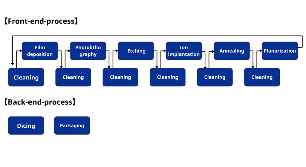
Semiconductor front-end and back-end process flow
Deposition, the process of creating a film using atoms, is...
Inside a semiconductor chip, circuits are formed by stacking various functional layers, such as transistors and other elements, wiring to connect them, and insulating layers for electrical isolation. The first step in forming this layered structure is deposition.
Thin-film deposition is a process of depositing a material as a thin film onto the surface of a silicon wafer. In semiconductor manufacturing, this film is extremely thin, ranging from a few nanometers to tens of nanometers in thickness, and is formed by atoms and molecules adhering to and accumulating on the surface.
The key to this process is forming a thin, uniform film. If the film thickness varies from place to place, or if the film is distorted, it can lead to inconsistencies in transistor operation. Furthermore, if the film is non-uniform, it will affect the interface with the substrate, making it more susceptible to defects.
Furthermore, since transistor operation is highly dependent on film thickness, even slight differences in film thickness can alter performance. Recent advancements in semiconductor miniaturization have resulted in device dimensions on a nanometer scale, requiring the films to be formed extremely thin to accommodate this.
There are various methods for thin-film deposition, but the following techniques are mainly used in semiconductor manufacturing.
What are thin-film deposition methods? Differences between PVD, CVD, and ALD.
PVD(Physical Vapor Deposition)
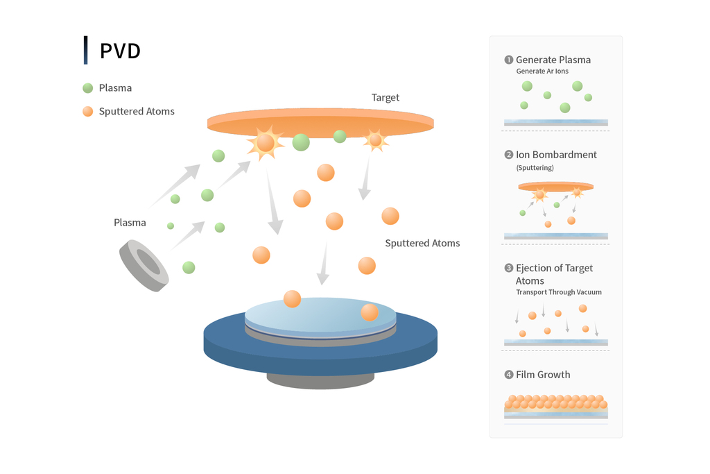
How PVD (Physical Vapor Deposition) works
PVD (Physical Vapor Deposition) is a method of depositing materials onto a wafer surface by physically evaporating and scattering them. A typical method is sputtering. It is widely used for forming metal films and is characterized by its relatively simple equipment structure. On the other hand, because the particles travel in a straight line, it can be difficult to form a uniform film deep into fine structures.
CVD(Chemical Vapor Deposition)
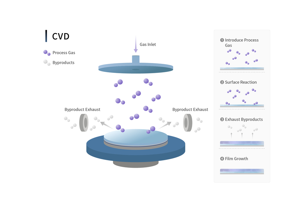
How CVD (Chemical Vapor Deposition) works
CVD (Chemical Vapor Deposition) is a method of forming a solid film on a wafer surface by reacting a gaseous precursor gas. Because the film is formed through a chemical reaction, it is relatively easy to form a uniform film, and it is used for depositing films of various materials. However, it is often a high-temperature process, so the impact on the material and substrate must be considered.
ALD(Atomic Layer Deposition)
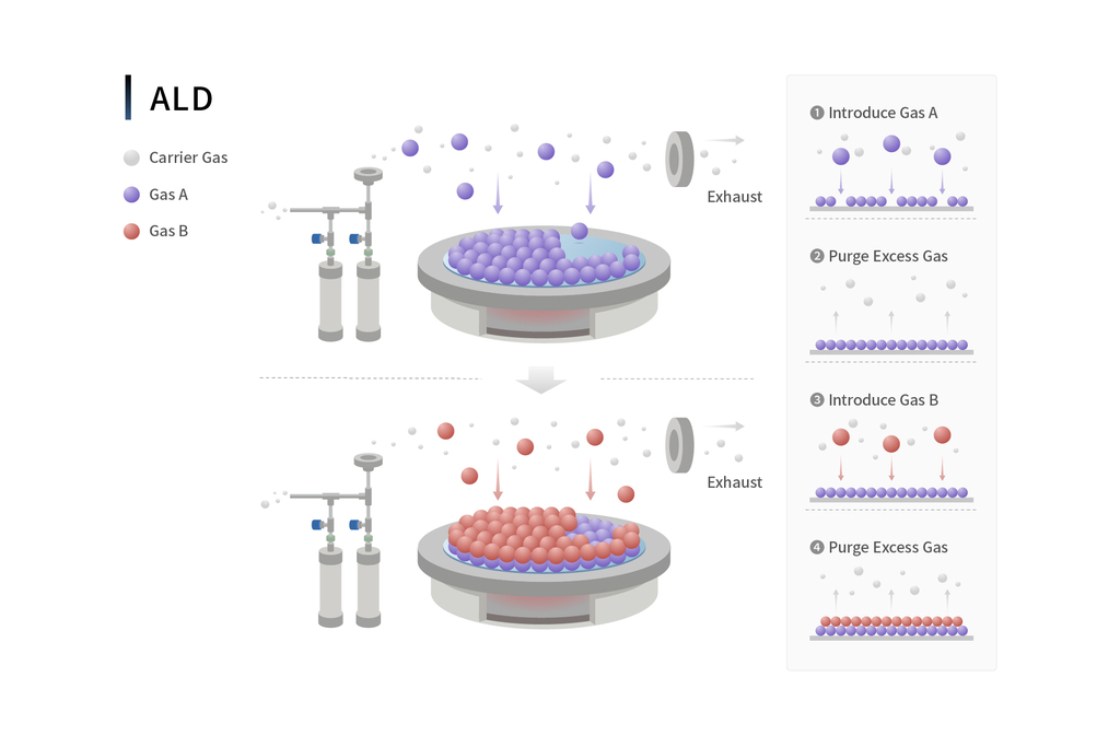
How ALD (Atomic Layer Deposition) works
ALD (Atomic Layer Deposition) is a method for forming films by controlling chemical reactions at the atomic layer level. By proceeding with the reaction step by step, extremely high film thickness control and uniformity can be achieved. Because it can form films uniformly even inside fine structures, it has become an important technology in cutting-edge semiconductor processes. On the other hand, it is characterized by a relatively slow film deposition rate.
Challenges related to thin-film deposition materials and miniaturization.
A wide variety of materials are used in the semiconductor film deposition process. Typical examples include silicon dioxide (SiO₂) and silicon nitride (Si₃N₄), which are used as insulating films, and tungsten (W) and copper (Cu), which are used for wiring and electrodes. High dielectric constant materials (such as HfO₂) used to improve transistor performance, and TiN and TaN, which are used as barrier materials for wiring layers, are also important materials.
As semiconductors become smaller, the performance requirements for these materials are also becoming more sophisticated. Film thicknesses have become as thin as a few nanometers, and not only the properties of the material, but also the atomic-level structure and interfacial reactions now have a significant impact on device performance.
Therefore, in recent years, material simulations, which can analyze material structure and surface reactions at the atomic level, have come to play an important role as a means of understanding these phenomena.
Examples of material simulations performed during film deposition
Now, let's look at some typical examples of the types of simulations that are performed.
① Analysis of reaction pathways on the substrate surface
In ALD, film deposition is carried out by chemically reacting precursors, such as organometallic compounds, on the substrate surface. Therefore, understanding the surface reaction mechanism at the molecular level is crucial for designing efficient precursors. For example, one example using Matlantis [ref] is a simulation of the reaction pathway between a hydrogen-terminated Si(111) surface and a cobalt precursor. This analysis visualized that the actual reaction proceeds through a two-step process: "surface bonding of Co atoms" and "desorption of hydrogen and allyl groups."
Furthermore, by using simulations to evaluate molecules that adsorb only to specific surfaces, it is possible to apply this technology to more advanced process development, such as the search for precursors for Area-Selective ALD (AS-ALD).
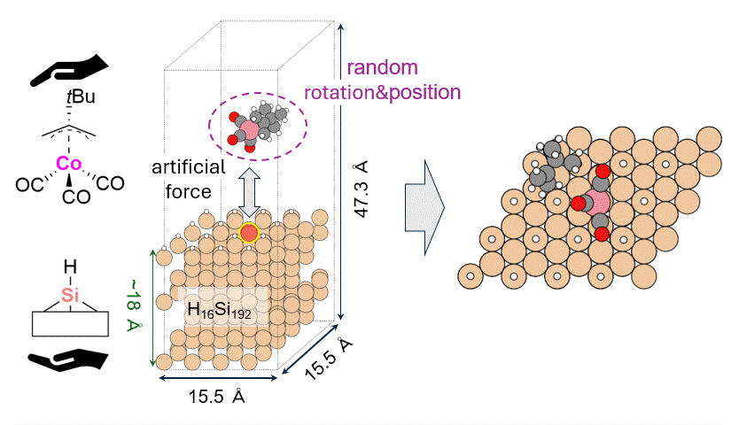
Structural model used in MC-AFIR calculation and obtained EQ. (Source: https://matlantis.com/en/calculation/analysis-of-urface-reaction-mechanism-between-ald-precursor-and-substrate/)
Photolithography is a technique for transferring circuit patterns.
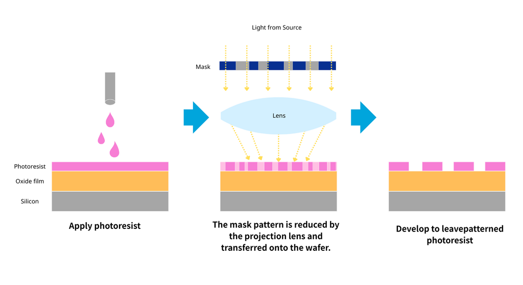
Photolithography is a process for forming semiconductor circuit patterns on wafers. By using light to transfer circuit patterns, nanoscale microstructures are created. Specifically, a photosensitive material called a resist is applied to the wafer surface, and light is shone through a mask to form a resist shape corresponding to the circuit pattern.
In recent years, photolithography technology has also evolved significantly in semiconductor processes, with the introduction of exposure techniques using extreme ultraviolet (EUV) light. As miniaturization progresses, many technological elements, such as optical design, resist material properties, and process condition optimization, are being controlled with high precision.
In particular, in EUV lithography, "metal resists" with a backbone of tin (Sn) or other materials that efficiently absorb light are attracting attention as next-generation materials [1]. Material simulation is key to exploring complex metal complexes. While the light absorption phenomenon itself is within the realm of quantum chemical calculations, material simulation is powerful for large-scale thermal and structural dynamics that affect the quality of the final pattern, such as "uniform film formation during coating," "crosslinking reactions associated with heating after exposure (PEB)" [3] and "interfacial phenomena with the developer" [4]. In fact, efforts are underway to construct probabilistic lithography models based on the chemical and material processes of metal oxide resists and compare them with experimental data [5]. Visualizing the complex reactions of the entire process at the nanoscale has the potential to accelerate resist development.
Etching is the process of removing unwanted material.
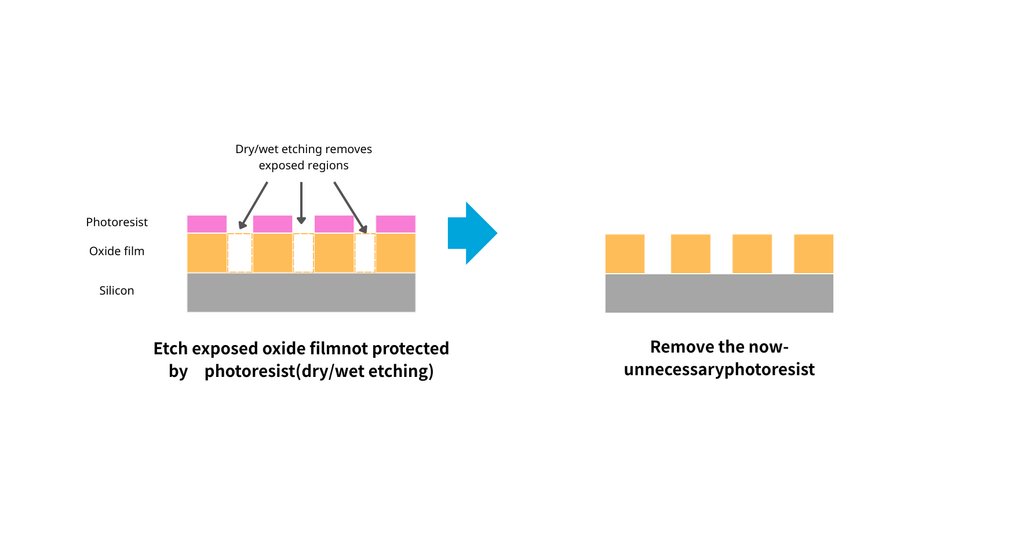
Etching is a process that removes only the unwanted parts of the material formed on a wafer. By using a resist pattern created by photolithography as a protective film and removing the surrounding material while leaving the resist pattern intact, a circuit pattern is formed on the wafer.
Etching is a process for processing thin films formed by deposition, and when used in combination with photolithography, it creates the fine structures of semiconductor circuits. Etching employs two main techniques: wet etching and dry etching.
Etching Methods: The Difference Between Wet Etching and Dry Etching
Wet etching
Wet etching is a method of removing material by chemically dissolving it using liquid chemicals. It is a relatively simple process and is characterized by its ability to remove material uniformly.
On the other hand, because the reaction with the chemical solution proceeds in all directions—up, down, left, and right—it may not be suitable for applications requiring high-precision processing of fine patterns, as it can lead to over-removal. For this reason, it is currently used in limited applications in state-of-the-art semiconductor processes.
Dry etching
Dry etching is a method of removing material using gas instead of liquid. First, a gas appropriate for the film material to be processed is introduced into the apparatus, and electrical energy is applied to activate the gas. The gas then becomes a plasma state, generating highly reactive particles such as ions and radicals.
These particles react with the material surface, or ions collide with the substrate surface perpendicularly, causing the material to be eroded. Because material can be removed while suppressing lateral processing, it is possible to form nanoscale microstructures with high precision.
Therefore, dry etching is widely used in current semiconductor manufacturing.
Challenges of miniaturization and etching processes
As semiconductors become smaller, controlling the etching process is becoming increasingly difficult. At the nanometer level, the reactivity of each material, chemical reactions occurring on the surface, and particle behavior in the plasma all significantly affect processing accuracy.
Furthermore, precisely controlling the "etching selectivity"—the process of removing only certain materials while leaving others intact—is also a crucial challenge.
What is material simulation performed during etching?
In etching processes, ions and radicals generated in a plasma react with the material surface, removing material at the atomic level. However, because these reactions occur on nanoscale surfaces, it is not easy to understand the detailed mechanism through experiments alone.
Therefore, in recent years, research has been conducted using atomic simulations to analyze the mechanisms of surface reactions and material removal.
Typical simulation examples related to etching include the following:
② Dry etching of SiO₂
We successfully simulated the dry etching of SiO₂ using hydrogen fluoride (HF) gas in Matlantis. This simulation successfully reproduced the formation of etching holes on the surface in a large-scale system of approximately 72,000 atoms, a feat impossible to calculate using conventional methods (DFT). This large-scale simulation makes it possible to efficiently determine optimal process conditions such as gas composition and incident energy.
Structural changes in an SiO2 slab after HF gas collision (Source: https://matlantis.com/en/calculation/sio2-dry-etching-simulation-using-lightpfp/)
Ion Implantation: Controlling Electrical Properties
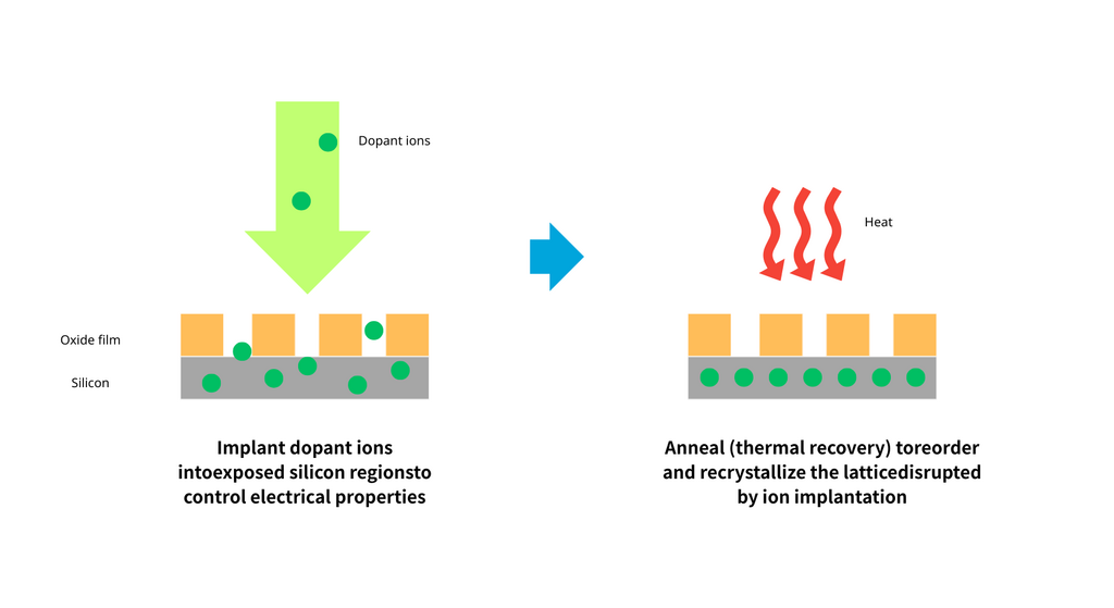
Ion implantation is a process that modifies the electrical properties of a silicon substrate by introducing impurity atoms (dopants). By accelerating ions such as boron (B), phosphorus (P), and arsenic (As) to high energy and implanting them into the wafer surface, an impurity distribution necessary for device operation, such as the source and drain regions and well structure of transistors, is formed. Immediately after implantation, the impurities do not function electrically and the crystal structure is destroyed, so annealing (heat treatment), which is performed as part of the process, is carried out to activate the impurities and repair defects.
In ion implantation and annealing, the distribution of impurities in the depth direction and the degree of recovery from damage to the substrate change depending on the energy, angle, and dose of the implanted ions, as well as the heat treatment conditions. As miniaturization progresses, control of impurity distribution at the nanometer level is required, making process optimization increasingly important.
In these processes as well, atomic-level analysis using material simulations is utilized. As shown in the ion irradiation simulation below (③), by tracking atomic displacement, cascade damage, the stopping position of the injected ions, and subsequent thermal diffusion when high-energy ions collide with the substrate using molecular dynamics calculations, it is possible to understand the details of processes that are difficult to observe directly in experiments.
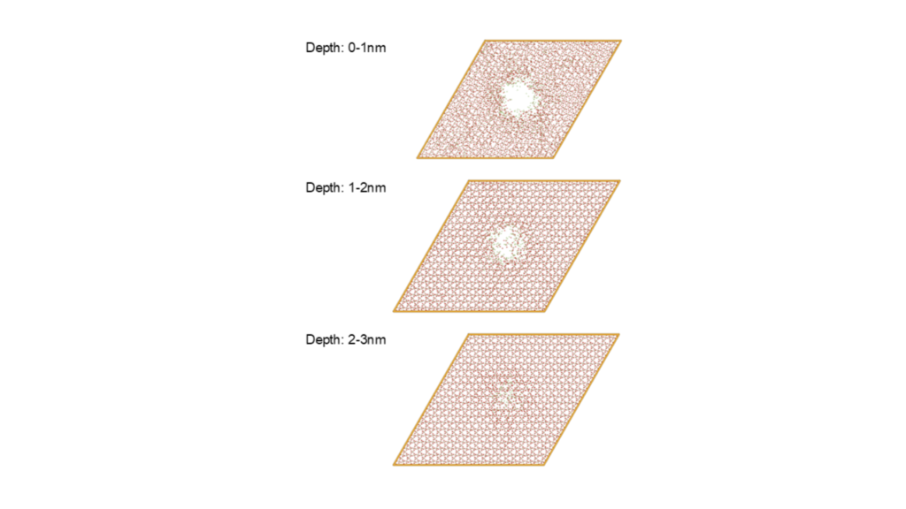
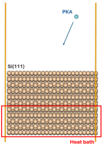
③ Ion irradiation simulation
Molecular dynamics (MD) simulations are used to understand the collision process between high-energy ions and material surfaces in dry etching. Matlantis allows for argon (Ar) irradiation simulations on Si(111) surfaces. By calculating non-equilibrium dynamics while varying the incident energy and angle, physical effects such as surface damage and atomic displacement due to ion collisions can be evaluated at the atomic level, leading to process optimization.
Simulation of Ar atomic irradiation on a Si surface (Source: pfcc-extras calculation example)
What is CMP, which flattens surfaces?
Inside a semiconductor chip, layers of transistors, wiring, and insulating films are repeatedly stacked through processes such as film deposition and etching. However, repeating these processes gradually creates irregularities on the wafer surface. If the surface irregularities become too large, the accuracy of the circuit pattern may decrease.
This is where the CMP (Chemical Mechanical Polishing) process comes in. CMP is a process that uses chemical and mechanical polishing to flatten the wafer surface. It removes irregularities in the layer structure formed by film deposition and etching, creating a state where circuit patterns can be formed with high precision in the next process.
In CMP, a wafer is pressed against a rotating polishing pad while polishing is performed using a polishing liquid called a slurry. The slurry contains polishing particles (abrasive grains) and chemicals that promote chemical reactions. The material surface is softened through chemical reactions, and then gradually abraded by mechanical friction. By combining these chemical and mechanical actions, it becomes possible to flatten the surface with nanometer-level precision.
CMP plays a crucial role not only in polishing but also in the formation of metal wiring layers. For example, in the copper wiring process, after embedding copper in the wiring grooves, excess copper is removed by CMP to form the wiring structure.
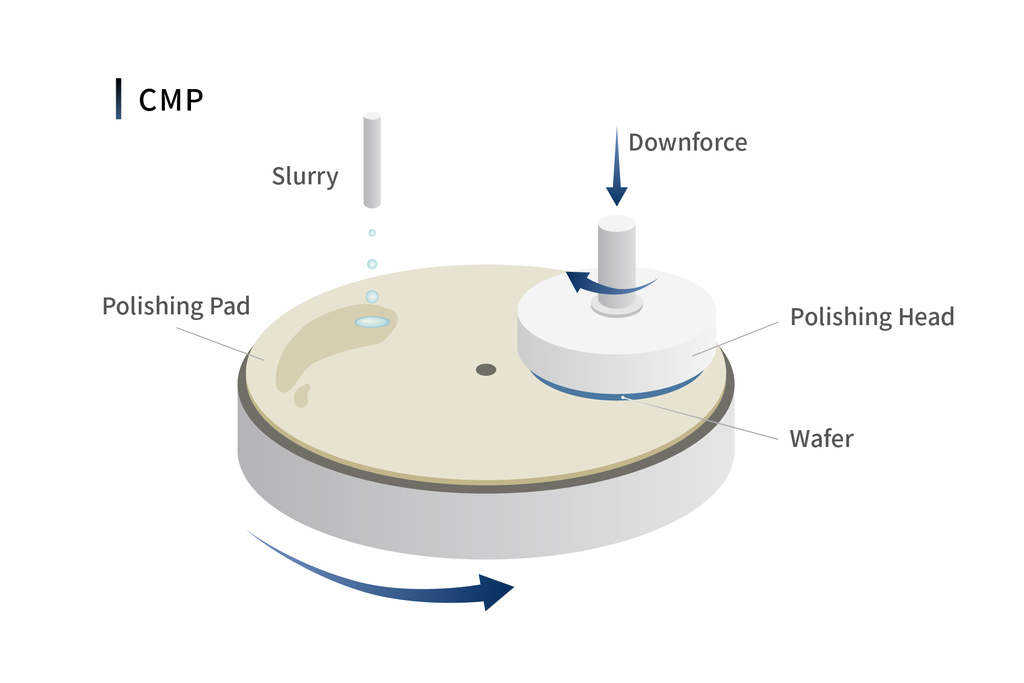
Overview of CMP (Chemical Mechanical Polishing)
Challenges of the CMP Process
As semiconductors become smaller, controlling the CMP process is becoming increasingly difficult. For example, because polishing rates differ depending on the material, problems can arise where some materials are polished too much. These phenomena can affect the reliability and electrical properties of the wiring.
In CMP, the interactions between the polishing pad, slurry particles, and the material surface are complex. Many parameters, such as the size and concentration of polishing particles, the progress of chemical reactions, and mechanical friction conditions, affect the polishing results, making the optimization of process conditions a crucial challenge.
Material simulations performed in CMP
Research utilizing material simulations is also progressing in the CMP process. For example, studies are being conducted to understand differences in polishing speed and selectivity by analyzing at the atomic level the interaction between particles in the polishing slurry and the material surface, as well as the material removal mechanism due to chemical reactions on the surface.
④ Molecular dynamics simulation of Si polishing with SiO₂ particles
This analysis models the actual polishing process by applying a vertical load and a horizontal driving force to SiO₂ particles and moving them across the substrate. The calculations confirmed that a larger driving force resulted in the removal of more Si atoms.
Notably, this trend is consistent across both Matlantis' standard model (PFP) and its computationally cost-effective lightweight model (LightPFP), demonstrating that the polishing process can be reproduced using LightPFP as well.
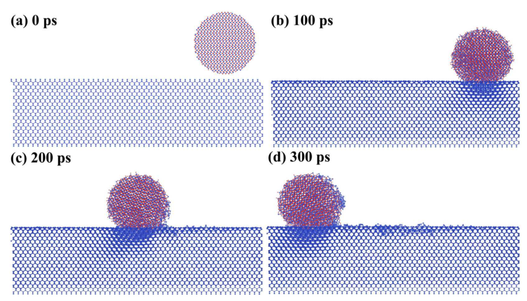
CMP MD simulation example (Source: https://arxiv.org/abs/2510.23064)
Cleaning that controls surface condition
In semiconductor manufacturing, cleaning processes are repeatedly performed before and after each step, such as film deposition and etching. Cleaning is not merely about removing contaminants; it plays a crucial role in removing particles, organic residues, and metallic impurities, and creating an interface suitable for the next process.
There are two main types of cleaning processes: wet cleaning and dry cleaning. Wet cleaning, which removes contaminants using chemical solutions, offers high cleaning efficiency. However, in highly refined pattern structures, surface tension during the drying process can cause structural deformation or collapse (pattern collapse). Therefore, in recent years, the importance of dry cleaning using plasma or gas reactions, and process designs that reduce the effects of surface tension, has been increasing.
Furthermore, it is known that cleaning conditions can alter the removal of oxide films and the surface termination state, affecting subsequent initial film growth, interface state density, adhesion, and contact resistance.
Thus, the cleaning process involves not only residue removal but also multiple atomic-level phenomena such as adsorption and desorption reactions, surface termination formation, and even microstructure stability. In recent years, material simulations have been increasingly used to understand and optimize these processes.
Examples of research and development utilizing materials simulations by companies
With the increasing miniaturization of semiconductor devices, controlling film thickness by several nanometers and differences in interface structure now significantly impact device performance and yield. Therefore, understanding atomic-level material behavior, such as surface reactions, defect generation, diffusion, and interface formation, is becoming increasingly important in process development.
Because many of these phenomena are difficult to observe directly through experiments alone, efforts to analyze reactions and structural changes occurring during processes using material simulations are becoming widespread. In recent years, the ability to perform large-scale and high-speed atomic simulations has enabled applications in comparing process conditions and designing materials, which were previously difficult.
I will now introduce some examples of research papers that specifically utilize simulations in semiconductor research and development.
[Case study provided by: SCREEN Holdings Co., Ltd.] Data-driven search for low-adsorption energy molecules on Si surfaces using molecular calculations and machine learning.
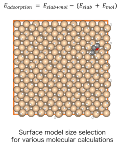
Schematic diagram of the H-terminated Si surface model.
In semiconductor manufacturing, a high degree of cleanliness is required, meaning no residue is left on the Si substrate surface. Therefore, the search for new chemical candidates is ongoing. However, evaluating a vast number of candidate materials through experiments alone is not easy.
This case study introduces a data-driven method that combines atomic-level simulations using Matlantis with machine learning to efficiently search for promising molecules using adsorption energy to Si surfaces as an indicator. This approach narrows down candidates for experimental verification from a vast material space.
Click here for case details.
Reaction analysis of TMA in a system that mimics the surface of silicon oxide film
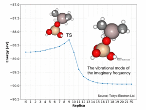
In semiconductor manufacturing processes, understanding the reaction mechanism between the film deposition precursor and the substrate surface is crucial for material selection and process optimization. However, performing reaction analysis on solid surfaces using DFT calculations requires significant computational resources and time.
In this case study, we analyzed the reaction pathway of trimethylaluminum (TMA), a widely used ALD precursor, in a system simulating a silicon oxide film surface using Matlantis. This demonstrates the potential for screening multiple candidates within a realistic timeframe, while evaluating activation energies with accuracy comparable to DFT calculations using NEB calculations.
Click here for case details.
References
[1] S. Kim et al., “Organometallic and coordinative photoresist materials for EUV lithography and related photolytic mechanisms,” Coordination Chemistry Reviews, vol. 493, 215307, 2023.https://doi.org/10.1016/j.ccr.2023.215307
[2] S. Grzeskowiak et al., “Multinuclear Tin-Based Macrocyclic Organometallic Resist for EUV Photolithography,” ACS Applied Materials & Interfaces, 2024.https://pmc.ncbi.nlm.nih.gov/articles/PMC11393934/
[3] D. Kim et al., “Computational approach on PEB process in EUV resist: multi-scale simulation,” Proc. SPIE, vol. 10143, 2017.https://doi.org/10.1117/12.2258029
[4] J. Lee et al., “Coarse-Grained Modeling of EUV Patterning Process Reflecting Photochemical Reactions and Chain Conformations,” Polymers, vol. 15, no. 9, 2023.https://pmc.ncbi.nlm.nih.gov/articles/PMC10180770/
[5] C. D. Needham et al., “Advanced simulations using an improved metal oxide photoresist model,” Proc. SPIE, vol. 12957, 129571B, 2024.https://doi.org/10.1117/12.3010941
-


 URL
URL
Copied
Latest Articles
NEW
Micro-Physical AI: The Atomic-Scale Frontier of Physical AI and the Future of Materials Discovery

CEO Blog

NEW
What is lab automation? Concepts and latest trends in experimental automation in materials development.

Lab Automation Explainer

From Lab to Deployment: Three Computational Trends Shaping the Future of Industry at TechConnect 2026

Conference Report
Three Computational Trends Reshaping Materials Science from TMS 2026

Conference Report

What Is Digital Transformation in Materials R&D? Accelerating Materials Discovery
Materials Informatics computational chemistry